For
very high speed mixed-signal ICs for test instruments and and 40-100G
Transimpedance Amplifier (TIA) for optical fiber communication
applications, two generations (5 processes) of InP HBT technologies have
been developed with ƒT from 110 GHz to 330 GHz. Superior performance
has been demonstrated by customers and several has been in production
since 2007.
HBT Parameters
Units
DHBT1
DHBT2
DHBT3
DHBT3B
DHBT5
Emitter width
(um)
1
0.8
0.8
0.6
1.6
Typical operating current density
Jctyp (mA/µm2)
1
2
2
2
1
Maximum operating current density
Jcmax (mA/µm2)
2
3
3
3
1.5
Typical operating voltage
Vce (V)
1.5
1.5
1
1
3.5
Base-collector breakdown voltage
BVcbo (V)
8
5.5
4.5
4.5
15
Collector-emitter breakdown voltage
BVceo (V)
7
4.5
3.8
3.8
11
Emitter-base breakdown voltage
BVbeo (V)
3.2
3.2
3.2
3.2
3.2
Thermal resistance
Rth (°C/mW)
3
5.3
5.3
5.3
2
ƒT (at max allowed operating current)
(GHz)
150
240
290
320
110
ƒmax (at max allowed operating current)
(GHz)
180
200
250
330
150
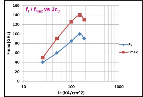
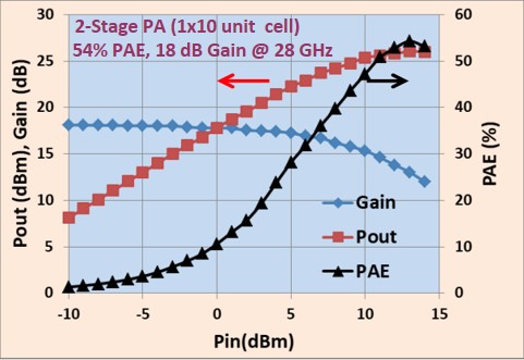
DHBT5
DHBT5 InP HBT technology is ideal for 5G PA applications at mm-wave frequency
High breakdown voltage
High power density, high gain and efficiency, good linearity